 1999, First-Grade Homework")

Tektronix sent me a new TDS2024C! Now what do we do with new $1500 toys?
WE RIP THEM APART (⌐■_■)っ═一
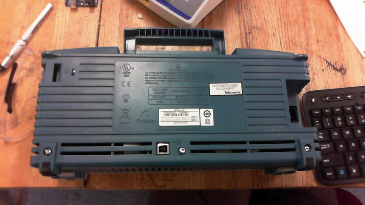 Let’s look at her from behind. Not much going on there, apart from a USB device port, FCC information, a kensington lock and various certification info. All and all, pretty boring.
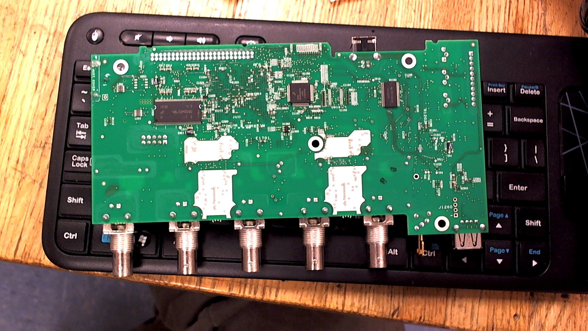
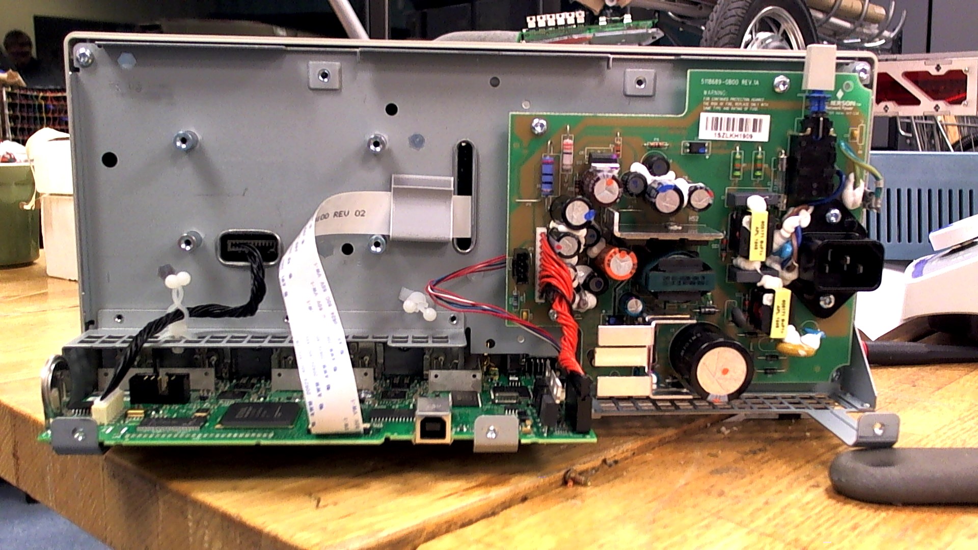 However inside it’s still pretty boring! There’s a power supply, a mainboard, a ribbon for the display panel and a wire harness for the human interface panel.
The power supply itself is noteworthy though. Interestingly enough it’s all through-hole constructed, on a single sided PCB. Like most SMPS’s, it’s a flyback converter, and a very well filtered one at that (second order LC on the input). Everything is well-glued, isolation slots are properly routed, what needs cooling is heatsinked well and overall, it’s a very nice power supply. The switch is hefty, and the IEC connector is nicely screwed into a big metal frame.
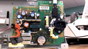 I don’t see this failing anytime soon. Though it doesn’t mean much to anyone looking to buy one [it’s custom], it’s an Emerson Networks 7001574-J100 power supply, Rev 1A. It’s output voltages are: -4.22V, +3.3V and +5.8V. Some of these are odd voltages, but I know exactly why they’ve chosen them…
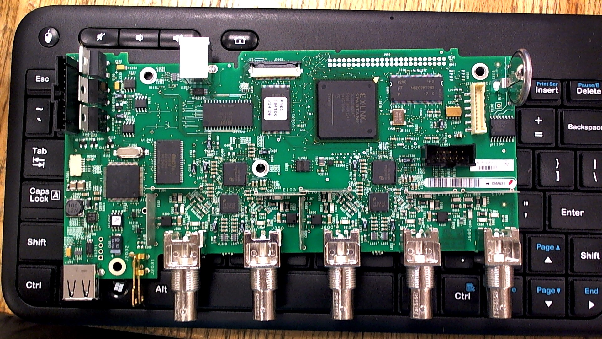 …Take a look in the top left corner of the mainboard: there’s a whole bunch of linear regulators! Specifically, a circuit that has a 0.7V intrinsic potential loss, hence the 5.8V supply for this board. There’s also a negative voltage source on there, similarly, only a few tenths of a volt below what’s fed to it. One might wonder why these are even here.
Two words; noise floor. In a scope it must be as low as possible, and the way you do that is through linear regulation, and active filtering.
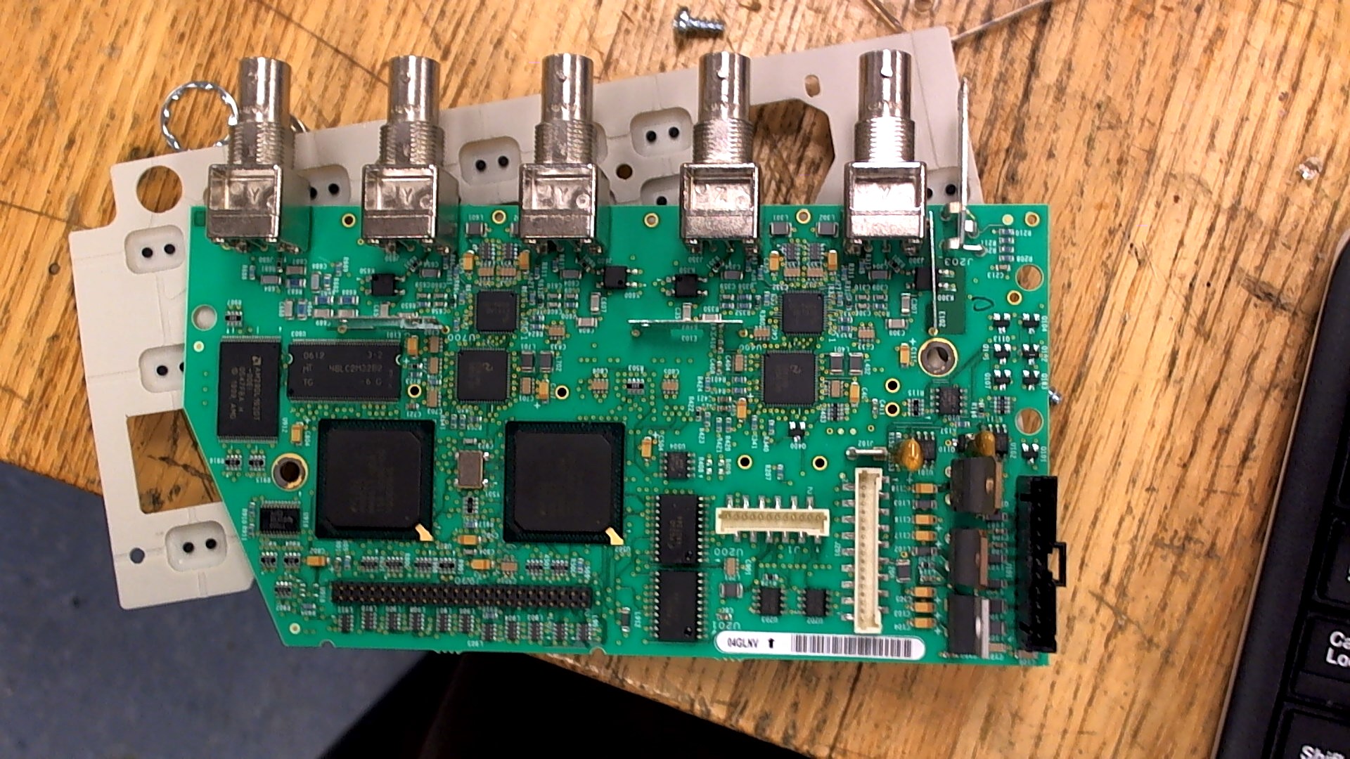
What else is on this board though?
Well…
 * A Xilinx Spartan FPGA
* Firmware EEPROM’s
* Several megabytes of asynchronous RAM (71v016sa12bfg) for the sample memory.
* A pair of custom ASICs, marked 32zcc87639858-00. I’m assuming these are what do the signal analysis for each channel pair.
* Another pair of custom ASICs, marked 31zceg79857-00. Without doubt these are the analog front-ends/daqs, which handle all of the level shifting, attenuation and signal sampling.
* A CY7C67300, “EZ-Host” embedded USB host controller, from cypress logic. This looks like an interesting IC…
* A DS1339C, I2C Real time clock IC, and associated CMOS battery. This is a data-logging scope, so it makes sense that it should know what time it is!
* A pair of 48lc2m32b2 62MB SDRAMs from Micron, likely the system memory.
* An AC16244, which seems to be a mysterious TI ASIC. And last but not least…
* A freescale MC6800 processor! (on back). This is really the main system chip: an 8-bit microprocessor from the 70’s.
What the heck?
Evidently it was fast enough to run the LCD display. Or not; that’s probably the FPGA’s job. Still though, why would anyone in this day and age where 32 bit ARMs are $5 each, use a 6800 in an oscilloscope of all things? Was it because they were military approved? Or was that just lazy engineering? I’d appreciate it if someone could shed light on that.
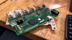
For comparison, here’s the TDS2024A’s mainboard. It hasn’t changed much.
Interestingly enough, this board has no EMI shielding. At all. There are some little castle-wall plate type things, but I’d be shocked if those actually did anything. Not only that, but there’s no metal enclosure around any of this circuitry; not even metallized plastic. Essentially, all of these signal paths are wide open for the world to see, and thus open for ambient RF to come and screw things up. Noticeably, too: turning on my Metcal near this scope increases the noise floor by almost 20mV!
Not good.

On the front panel there’s nothing special: buttons, LEDs, rotary encoders and an LED backlit display. Interestingly enough though, this is an IPS display. For those who don’t know, IPS, or in-plane-switching, is a type of LCD technology that allows for excellent color rendition, ultra-wide angle viewing and an all-around better LCD experience. It’s actually a huge improvement over past models, if you ask me.
Overall,
I give the scope a 6/10.
On the plus side, the tektronix UI is as simple and elegant as ever, and the scope is a joy to use. The FFT function is much-improved, there’s a crap-ton of measurement and data logging features, and the ability to save waveforms to flash is very useful when archiving reference signals.
However, -1 points for not having a reasonable sample depth: 10kpoints is just not enough in these days of cheap RAM. -0.5 points for not having a modern processor, and another 0.5 points for a USB host that can’t understand more than 2GB of flash memory. Lastly, minus another 2 points for no EMI shielding. That’s really a pain in the ass when working with RF and power electronics, and I had to add it myself for that purpose!
That’s not to say I’m complaining; thank you tektronix, for doing what you could to make a customer happy. But, it’s high time for some innovation in those engineering labs if you want to stay on top!
Read
hi,I am a physics sntedut with some experience with electronics. I have ordered parts for the ZVSdriver you are using.I have a question about the toroidal inductor. I have some ferrite toroids laying around I pulled from computermonitors while getting their flybacks. I don’t know how to look up their characteristics to calculate the inductance. In the past I tried using a bridge and Oscope, but that has not worked well for me.Is there a rule of thumb that will get me moderate enough accuracy to make a good circuit ?The flyback I have choosen puts out a strong arc with my 555 driver. More so than another larger looking FB.My MMC kinda sucks since I didn’t figure what to buy until after I spent some money, so I need to break (use) what I have first; 50, 2KV ceramic 0.01uF caps, 10 series = 1nF with a max of 5nF.As well, I don’t have 2W resistors but do have 1W resistor .hoping that will work enough to get startedespecially since I can only draw 5 A from my supply.I’d love to make my own power supply. I have tried to make a small one for practice but the loading is confusing me. I started with 35 Vpp and by the time it as rectified and had a large cap in parallel, it was down to 3 VDC. I would prefer to make it regulated. I had an electronics lab which built a Wilson mirror and a BJT voltage. Do you have a link to a good schematic or can I use yours ?thanks for reading all this cheers,wbg